This thesis focuses on developing novel components for cryoelectronics applications, particularly aiming to realize controllable nanometer-thin tunnel barriers between metal and semiconducting layers. This involves the growth of thin films of dielectric, such as silicon nitride, onto the surface of a silicon wafer.
The research is conducted within the clean room facility at VTT Technical Research Centre of Finland Ltd., which is equipped with a LPCVD furnace capable of depositing silicon nitride. Additionally, a direct thermal growth method is investigated, aiming to achieve ultra-thin layers of silicon nitride. The direct thermal method is tested by using two sets of wafers: one subjected to standard RCA cleaning process and the other undergoing an extra dip with HF after the standard RCA. This distinction in surface treatment is crucial with respect to the removal the native uniform silicon oxide layer from the thin films, thereby influencing the properties of the deposited layers.
Silicon nitride (Si3N4) is well regarded as an electrical insulator owing to its superior diffusion barrier properties compared to silicon dioxide (SiO2). This popularity arises also from its effectiveness in mitigating corrosion and alkali contamination in microelectronic devices. Its notable characteristics, including high resistivity (up to approximately 1015 Ωcm) and dielectric strength, render SiN one preferred choice for insulation purposes. Si3N4 is also utilised in high-voltage insulation applications, such as power distribution systems and electrical transformers, to offer dependable electrical insulation even at high voltages.
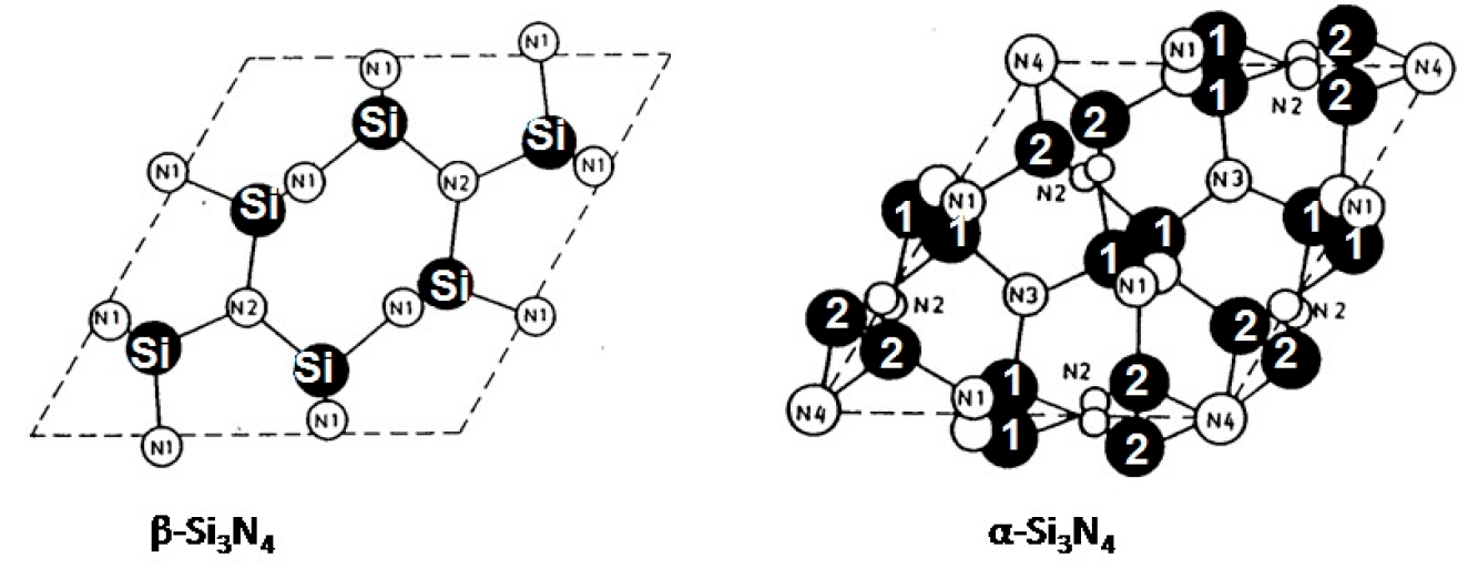
Fig. 1 shows the crystalline structure of α − Si3N4 and β − Si3N4. Trigonal α − Si3N4 has lattice constants a=775.193(3) pm and c= 561.949(4) pm, and the space group is P31c(159). Hexagonal β − Si3N4 has a=760.8 pm and c= 291.1 pm, with a p63/m space group. According to Fig. 1, the structure consists of corner-sharing SiN tetrahedra, which shows ABCDABCD... arrangement and ABAB... arrangement for N and Si layer configuration for α and β, respectively.

Figure 1. Hexagonal and trigonal silicon nitride (Black circles:Si / White Circles:N)
Si3N4 has a relatively high melting point compared to other materials, which adds to its stability and utility in various applications. The melting point varies according to the composition and production procedure, although it usually ranges between 1,800 and 1,900 degrees Celsius. Its high melting point enables it to survive the high temperatures required in semiconductor processes, such as Chemical Vapor Deposition (CVD) and sintering, annealing, without deteriorating or changing phase.
CVD is widely utilized in thin film fabricating industries. The advantages of CVD are that it can be used to coat many wafers simultaneously. It can be executed under elevated pressures where the mean free path for gas molecules becomes significantly reduced. Additionally, the utilization of relatively high temperatures is distinctive feature.
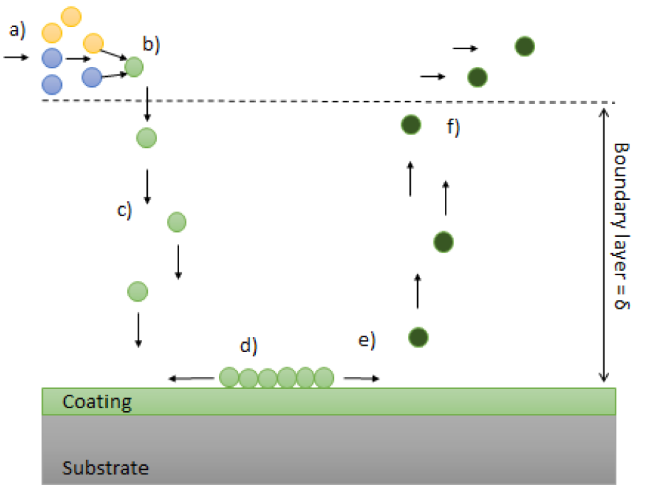
Numerous steps characterize the CVD process, as depicted in Fig. 2. a) Precursor gases are introduced into the chamber, b) chemical reactions occur among the precursor gases, c) the gases diffuse through a boundary layer, d) they undergo deposition onto the surface, e) product gases desorb from the surface, and f) they are evacuated from the chamber through pumping.

Figure 2. CVD reaction process
There are many CVD types used for thin film fabrication. LPCVD, Atmospheric pressure chemical vapor deposition (APCVD) and Plasma enhanced chemical vapor deposition (PECVD) are major CVD processes. However, the fabrication method differs between several factors, namely sample temperature, mechanical morphology, electrical and chemical properties, deposition rate and film uniformity.
The typical LPCVD reactor, commonly referred to as a vertical furnace, is depicted schematically in Fig. 3. This reactor comprises a lengthy vertical quartz tube capable of accommodating as many as 150 wafers. The boat which is used to load the wafers is manufactured from silicon carbide or quartz glass. By maintaining the distance in between each wafers around few millimeters, samples are loaded to the boat. The particular pitch is selected by the initial structure of the design of LPCVD furnace. The boat is placed into the LPCVD furnace and then the reactor environment is sealed. Large resistive heater elements are employed to heat the system surrounding the reactor. Uniformity of temperature is an important process goal, and it is managed by controlling the heating in five zones along the length of the reactor. This control, with an accuracy of ±1 °C ensures process homogeneity and reproducible across all treated wafers during the LPCVD process.

Figure 3. Schematic diagram of a vertical LPCVD furnace
While LPCVD is a deposition method, direct thermal nitridation is a growth process. Thermal nitridation is a process where a material, often a metal or semiconductor, is exposed to high temperatures in a nitrogen-rich environment, forming a nitride layer on its surface. The amount of silicon nitride formation via thermal nitridation depends on several factors such as temperature and duration of the nitridation process.
上一篇: 硅孔光学器件