Two-dimensional (2D) semiconductors, particularly transition metal dichalcogenides, exhibit high mobility within atomic-scale thickness, immunity to short-channel effects, and back-end-ofthe-line (BEOL) compatibilitywith complementary metal-oxide-semiconductor (CMOS) technology. These attributes have sparked substantial interest in extending the semiconductor roadmap beyond silicon. Major companies including TSMC, Intel, Samsung and IMEC have allocated substantial resources to research into, and development of, 2Dsemiconductor technology for advanced technology nodes. The identification of the present development stage and the future target is vital to expedite the transition of 2D semiconductor technology from laboratory to production line. This perspective aims to provide a concise survey of the current progress and future direction of high-performance field-effect transistors (FETs) and integrated circuits (ICs) based on 2D semiconductors.
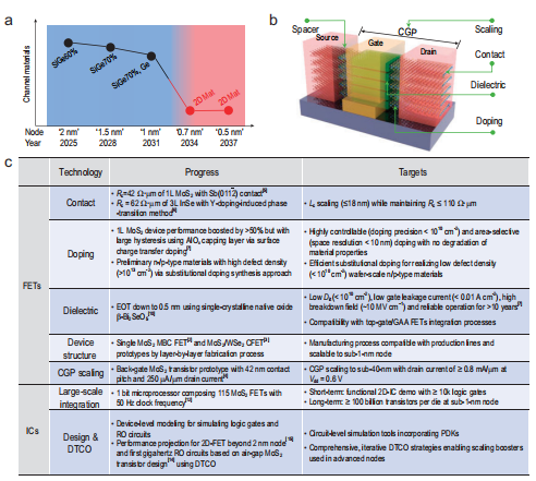
The International Roadmap for Devices and Systems (IRDS) projects the introduction of 2D semiconductors as channel materials in 0.7 nm nodes in 2034, in a highly scaled threedimensional (3D) device architecture (Fig. 1a). The basic building block comprises a vertical complementary field-effect transistor (CFET) with gateall-around (GAA) geometry (Fig. 1b), featuring a gate length of 12 nm and contacted gate pitch (CGP) of 38 nm . Here, CGP denotes the minimal separation between neighboring device gates. Prototype devices, such as multibridge channel (MBC) FETs, CFETs utilizing 2D semiconductors , and MoS2 back-gate FETs with a contact pitch as small as 42 nm, have been reported. However, their fabrication processes present challenges for scalable and CMOS-compatible production, and their device performance falls short of the IRDS requirements due to unresolved issues in metal contact, dielectric integration, doping, spacer design, etc.

Figure 1. (a) Evolution roadmap ofchannel materials based on IRDS 2022. (b) Schematicrepresentation of an ideal nanosheet FET highlighting key technologies. (c) Significant advancements and challenges in 2D semiconductor devices and integrated circuits.
In silicon CMOS, the contact and spacer regions undergo heavy doping with a concentration ranging from 10to 10cm−3 to reduce access resistance while keeping parasitic capacitance low, thereby reducing the resistive-capacitive (RC) delay of the transistor . Consequently, it is imperative to develop controlled and reliable doping techniques for constructing transistors and ICs using 2D semiconductors. Currently, the most promising doping methods include substitutional doping and surface charge-transfer doping. Substitutional doping involves the addition of external donor or acceptor elements during material synthesis, which has the potential to produce p- and n-type materials in batch fabrication. However, the reduced screening in 2D semiconductors leads to much larger dopant ionization energy, thus much lower doping efficiency than bulk semiconductors. Surface chargetransfer doping offers a gentle approach that preserves the structure of 2D materials. CMOS-compatible dopants mainly consist of non-stoichiometric oxides and nitrides, such as SiOx, AlOx, MoOx and SiNx. By employing photolithography, the spatially selective doping of 2D materials becomes achievable, and beneficial for realizing the ideal integrated device structure in Fig. 1b. Yet, these nonstoichiometric oxides might introduce additional long-range optical phonon scattering, and achieving precise control of the doping level remains challenging. Although the recently reported remote modulation doping method addresses this concern to some degree, it appears incompatible for device scaling. Reliable and effective doping methods for 2D semiconductors are still to be developed.
Although significant progress has been made in the performance enhancement of 2D transistors, the integration density of 2D ICs remains low. For example, a 1-bitmicroprocessor utilizingMoS2 transistorswassuccessfully demonstrated, featuring 115 transistors in an area of 0.6 mm2. In comparison, state-of-theart CMOS-based CPUs possess over 10 billion transistors in~100 mm2. This substantial gap is attributed to the immaturity of highly crystalline 2D semiconductor materials, the manufacturing process of device integration and circuit design environment (Fig. 1c). These areas all necessitate continuous research and development by academia and industry.
For materials, the production of large (up to 12-inch) wafer-scale singlecrystalline 2D semiconductor materials still poses a significant challenge, although proof-of-concept demonstration of 2-inch MoS2, MoSe2 and WS2 single crystals has been reported . Key considerations include meticulous substrate engineering, growth thermodynamics and kinetics, equipment design and process control. To achieve success in this field, it is crucial to engage in iterative processes throughout the growth process and prioritize the development of specialized equipment, distinct from the commonly employed tube furnaces found in academic laboratories. Besides, a viable wafer-scale, non-destructive transfer technology is required to relocate 2D materials from growth substrate to integration platform in an ultra-clean environment. Ideally, this technique should take place in a vacuum.
To facilitate the lab-to-fab transition of 2D semiconductors, there is an urgent need for the advancement of standard device-integration processes tailored for large-scale manufacturing. Besides the aforementioned issues, processes related to the interconnection/stacking of 2D semiconductor transistors and circuits must also be developed, including etching, vias, thin film deposition, atomic layer deposition/etching, chemical mechanical polishing, passivation and encapsulation. It is important to highlight that all of these processes must meet stringent requirements, including compatibility with CMOS technology, as well as the prevention of structural damage and interface contamination in 2D semiconductors. Adopting a more forward-looking viewpoint, it is possible that growth, fabrication, integration equipment and systems operating within a high-vacuum environment might ultimately evolve into the optimal solution for the future manufacturing of 2D semiconductor ICs.
Circuit design plays a crucial role in Very Large-Scale Integration (VLSI). While some efforts have been dedicated to device-level modeling, there remains a lack of comprehensive circuit-level simulation tools that incorporate process design kits (PDKs) to assess circuit performance. Additionally, although many studies have provided statistical information regarding yield and variability, it is important to establish clear definitions of yield criteria and acceptable variability windows. Furthermore, addressing the challenges faced by 2D semiconductors in VLSI requires more than just design-related solutions; it necessitates the adoption of a design technology co-optimization (DTCO) methodology. Recently, we adopted DTCO to report the first gigahertz ring oscillator (RO) circuits based on air-gap MoS2 transistor design. Looking forward, a process-aware DTCO approach is expected to yield a >40% improvement in the operating frequency performance of a 15-stage ring oscillator with a fan-out of 3 at 0.7 V supply in 2D-FET technology, as compared to silicon, at the IMEC2 nm node.